- 您现在的位置:买卖IC网 > Sheet目录2000 > IDTSSTE32882HLBBKG (IDT, Integrated Device Technology Inc)IC REGISTERING CLK DRIVER 176BGA
1.35V/1.5V REGISTERING CLOCK DRIVER WITH PARITY TEST AND QUAD CHIP SELECT
24
SSTE32882HLB
7201/14
SSTE32882HLB
1.35V/1.5V REGISTERING CLOCK DRIVER WITH PARITY TEST AND QUAD CHIP SELECT
COMMERCIAL TEMPERATURE
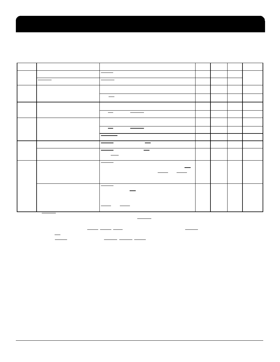
DC Current Specifications
Operating Electrical Characteristics
Symbol
Parameter1
1
The RESET and MIRROR inputs of the device must be held at valid voltage levels (not floating) to ensure proper device
operation. The differential inputs must not be floating unless RESET is LOW.
Conditions
Min
Typ2
2
All typical values are at VDD = 1.5V, TA = 25°C.
Max
Unit
II
Input current
RESET, MIRROR, VI =VDD or GND
±5
A
QCSEN input current
QCSEN, VI =VDD or GND
-150
5
IID
Input current
Data inputs3, VI =VDD or GND
3
DCKEn, DODTn, DAn, DBAn, DRAS, DCAS, DWE, DCSn, PAR_IN are measured while RESET is pulled LOW.
±5
A
CK, CK4; VI =VDD or GND
4
The CK and CK inputs have pull-down resistors in the range of 10K
to 100K.
-5
150
A
IOH
HIGH-level output current
Qn5
5
Qn = QxAn, QxCSn, QxCKEn, QxODTn, QxRAS, QxCAS, QxWE, and QxBAn.
-11
mA
Yn, Yn, FBOUT, FBOUT
-11
mA
IOL
LOW-level output current
11
mA
Yn, Yn, FBOUT, FBOUT
11
mA
ERROUT
25
mA
IDD6
6
The supply current is measured as the total current consumption on the AVDD, PVDD, and VDD supply current pins. Io = 0.
Static standby current
RESET = GND and CK = CK = VIL(AC)5
mA
Low-Power Static Operating
RESET =VDD and CK = CK = VIL(AC), MIRROR =
VDD, DCS[1:0] = [0,1]
15
mA
ICCD
Dynamic operating -- input clock
only; active outputs
RESET =VDD, MIRROR = VDD, VI = VIH(AC) or
VIL(AC), RC0[DBA0]=0, RC0[DBA1]=0, CK and CK
switching 50% duty cycle, IO = 0, DCS0 = L, DCS1 =
H. VDD = VDDMAX
68
A/MHz
Dynamic operating -- per each data
input
RESET =VDD, MIRROR = VDD, VI = VIH(AC) or
VIL(AC), CK and CK switching 50% duty cycle. One
data input switching at one half clock frequency, 50%
duty cycle; RC0[DBA0]=0, RC0[DBA1]=0, IO = 0,
DCS0 = L, DCS1 = H. VDD = VDDMAX
16
A/Clock
MHz/
D Input
发布紧急采购,3分钟左右您将得到回复。
相关PDF资料
IDTSSTE32882KA1AKG
IC REGISTERING CLK DRIVER 176BGA
ISD1750SYR
IC VOICE REC/PLAY 50SEC 28-SOIC
ISD5008EYI
IC VOICE REC/PLAY 4-8MIN 28-TSOP
ISL12008IB8Z
IC RTC I2C LO-POWER 8-SOIC
ISL12020MIRZ-T7A
IC RTC/CALENDAR TEMP SNSR 20DFN
ISL12022IBZ-T7A
IC RTC/CALENDAR TEMP SNSR 8SOIC
ISL12022MAIBZ
IC RTC/CALENDAR TEMP SNSR 20SOIC
ISL12022MIBZ-T7A
IC RTC/CALENDAR TEMP SNSR 20SOIC
相关代理商/技术参数
IDTSSTE32882HLBBKG8
制造商:Integrated Device Technology Inc 功能描述:IC REGISTERING CLK DRIVER 176BGA
IDTSSTE32882KA1AKG
功能描述:IC REGISTERING CLK DRIVER 176BGA RoHS:是 类别:集成电路 (IC) >> 时钟/计时 - 专用 系列:- 标准包装:1,500 系列:- 类型:时钟缓冲器/驱动器 PLL:是 主要目的:- 输入:- 输出:- 电路数:- 比率 - 输入:输出:- 差分 - 输入:输出:- 频率 - 最大:- 电源电压:3.3V 工作温度:0°C ~ 70°C 安装类型:表面贴装 封装/外壳:28-SSOP(0.209",5.30mm 宽) 供应商设备封装:28-SSOP 包装:带卷 (TR) 其它名称:93786AFT
IDTSSTE32882KA1AKG8
制造商:Integrated Device Technology Inc 功能描述:IC REGISTERING CLK DRIVER 176BGA
IDTSSTUB32866BHLF
功能描述:IC BUFFER 25BIT CONF REG 96LFBGA RoHS:是 类别:集成电路 (IC) >> 接口 - 专用 系列:- 特色产品:NXP - I2C Interface 标准包装:1 系列:- 应用:2 通道 I²C 多路复用器 接口:I²C,SM 总线 电源电压:2.3 V ~ 5.5 V 封装/外壳:16-TSSOP(0.173",4.40mm 宽) 供应商设备封装:16-TSSOP 包装:剪切带 (CT) 安装类型:表面贴装 产品目录页面:825 (CN2011-ZH PDF) 其它名称:568-1854-1
IDTSSTUB32S869AHLF
功能描述:IC REGISTERED BUFFER 150-TFBGA RoHS:是 类别:集成电路 (IC) >> 接口 - 信号缓冲器,中继器,分配器 系列:- 标准包装:160 系列:- 类型:转发器 Tx/Rx类型:以太网 延迟时间:- 电容 - 输入:- 电源电压:2.37 V ~ 2.63 V 电流 - 电源:60mA 安装类型:表面贴装 封装/外壳:64-TQFP 裸露焊盘 供应商设备封装:64-TQFP-EP(10x10) 包装:托盘 其它名称:Q5134101
IDTSSTUB32S869AHLFT
功能描述:IC REGISTERED BUFFER 150-TFBGA RoHS:是 类别:集成电路 (IC) >> 接口 - 信号缓冲器,中继器,分配器 系列:- 标准包装:160 系列:- 类型:转发器 Tx/Rx类型:以太网 延迟时间:- 电容 - 输入:- 电源电压:2.37 V ~ 2.63 V 电流 - 电源:60mA 安装类型:表面贴装 封装/外壳:64-TQFP 裸露焊盘 供应商设备封装:64-TQFP-EP(10x10) 包装:托盘 其它名称:Q5134101
IDTSSTVF16857AGLF
功能描述:IC DDR REGISTER 48-TSSOP RoHS:是 类别:集成电路 (IC) >> 接口 - 专用 系列:- 标准包装:3,000 系列:- 应用:PDA,便携式音频/视频,智能电话 接口:I²C,2 线串口 电源电压:1.65 V ~ 3.6 V 封装/外壳:24-WQFN 裸露焊盘 供应商设备封装:24-QFN 裸露焊盘(4x4) 包装:带卷 (TR) 安装类型:表面贴装 产品目录页面:1015 (CN2011-ZH PDF) 其它名称:296-25223-2
IDTSTAC9200X3NAEB1X
功能描述:IC AUDIO CODEC 2CH HD 32-QFN RoHS:是 类别:集成电路 (IC) >> 接口 - 编解码器 系列:- 标准包装:2,500 系列:- 类型:立体声音频 数据接口:串行 分辨率(位):18 b ADC / DAC 数量:2 / 2 三角积分调变:是 S/N 比,标准 ADC / DAC (db):81.5 / 88 动态范围,标准 ADC / DAC (db):82 / 87.5 电压 - 电源,模拟:2.6 V ~ 3.3 V 电压 - 电源,数字:1.7 V ~ 3.3 V 工作温度:-40°C ~ 85°C 安装类型:表面贴装 封装/外壳:48-WFQFN 裸露焊盘 供应商设备封装:48-TQFN-EP(7x7) 包装:带卷 (TR)